University of Cambridge researchers have engineered an atomically-precise ‘energy sandwich’ using vapour-growth techniques to control halide perovskite layers with unprecedented precision. This breakthrough, led by Professor Sam Stranks, solves the long-standing instability and control problems that have plagued these materials, paving the way for durable, high-performance solar cells, LEDs, and lasers that could be produced at scale.
For years, scientists have been excited about halide perovskites, materials that are not only cheaper than silicon but can also be tuned to capture more of the sun’s light. Imagine a solar panel that could be printed as easily as a newspaper yet outperforms the rigid, expensive silicon panels on rooftops today. That’s the perovskite promise. But why aren’t they everywhere? The answer has always been chaos at the atomic level. These materials were notoriously unstable, and scientists struggled to stack them in neat, functional layers—a crucial step for building efficient devices.
The University of Cambridge team has now brought order to this chaos. By abandoning the messy ‘solution processing’ methods of the past, they turned to a vapour-based technique, the same method used to manufacture the silicon chips in your phone and computer.
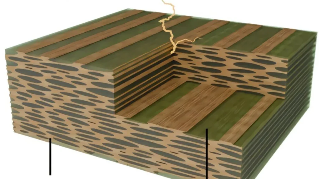
This allowed them to build their perovskite structures one atomic layer at a time, a process known as epitaxial growth. They combined three-dimensional and two-dimensional perovskites to create stacks where they could control the thickness of each film down to a fraction of an atom, reported the journal Science.
READ ALSO: https://www.modernmechanics24.com/post/nuclear-missile-aboard-french-navy-rafale
“A lot of perovskite research uses solution processing, which is messy and hard to control,” said Professor Sam Stranks from the Department of Chemical Engineering and Biotechnology, who co-led the research. “By switching to vapour processing — the same method used for standard semiconductors — we can get that same degree of atomic control, but with materials that are much more forgiving.”
What does this atomic-level control actually achieve? In a semiconductor ‘sandwich,’ each layer has a specific job: to guide electrons and their positive counterparts, called ‘holes,’ in the right direction. When these charges meet, they can either emit light efficiently or waste their energy as useless heat.
The Cambridge team discovered they could engineer the junctions between their ultra-thin layers to dictate this very outcome. They could create a junction that pulls the charges apart for solar cells or one that holds them together to emit light brilliantly for LEDs.
WATCH ALSO: https://www.modernmechanics24.com/post/china-humanoid-webster-stunt
“The hope was we could grow a perfect perovskite crystal where we change the chemical composition layer by layer, and that’s what we did,” said co-first author Dr Yang Lu from Cambridge’s Department of Chemical Engineering and Biotechnology and Cavendish Laboratory. “It’s like building a semiconductor from the ground up, one atomic layer after another, but with materials that are much easier and cheaper to process.”
The level of tunability the team achieved was startling, even to them. They found they could adjust the energy difference between the layers by more than half an electron volt. In some configurations, they extended the lifetime of the electric charges to over 10 microseconds—far longer than typically possible, which is vital for efficient light emission and conversion.
“We’ve reached a level of tunability that wasn’t even on our radar when we started,” said Professor Sir Richard Friend from the Cavendish Laboratory, who co-led the research. “We can now decide what kind of junction we want — one that holds charges together or one that pulls them apart — just by slightly changing the growth conditions.”
READ ALSO: https://www.modernmechanics24.com/post/china-unveils-as700-airship-in-shaoxing
This newfound precision is the key to moving perovskites from the lab bench to the marketplace. The ability to reliably build these ‘energy sandwiches’ using scalable vapour-processing methods means that the dream of cheap, highly efficient perovskite solar panels and ultra-bright, low-energy displays is now significantly closer to reality.
The team’s work demonstrates that perovskites can finally be tamed and integrated into the sophisticated, multi-layered architectures that power modern technology, according to Science.
“Changing the composition and performance of perovskites at will – and probing these changes – is a real achievement and reflects the amount of time and investment we’ve made here at Cambridge,” said Stranks. “But more importantly, it shows how we can make working semiconductors from perovskites, which could one day revolutionise how we make cheap electronics and solar cells.”
WATCH ALSO: https://www.modernmechanics24.com/post/mono-rail-arunachal-army-innovation-16000ft