We’ve grown accustomed to our gadgets shrinking while their power grows exponentially. But what happens when this relentless miniaturization, the very engine of the digital age, finally hits a wall? The laws of physics, after all, aren’t so easily bypassed. Scientists have been warning for years that we’re approaching a quantum mechanical limit, a point where making transistors smaller becomes astronomically expensive and physically problematic.
So, where do we go from here? If we can’t just keep making things smaller, the only logical direction is to start building up.
Imagine a bustling city that can’t expand its borders any further; the only way to grow is to construct towering skyscrapers. This is precisely the revolutionary approach a team from King Abdullah University of Science and Technology (KAUST) has just demonstrated, and they’ve shattered all previous records in the process.
Historically, the semiconductor industry’s mantra has been “smaller, faster, cheaper.” But as KAUST Associate Professor Xiaohang Li, the lead researcher, explains, that path is becoming a dead end. “We are reaching a quantum mechanical limit and the cost is skyrocketing,” he states. “To continue advancing, we must look beyond planar scaling; stacking transistors vertically is a promising solution.” Instead of a sprawling suburban layout of transistors, they’re building a dense, vertical metropolis for electrons.
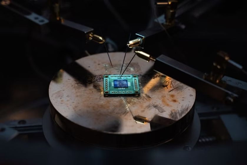
And what a metropolis it is. While the rest of the scientific community has struggled to create hybrid microchips with more than two stacked layers, the KAUST team has successfully built the world’s first six-stack hybrid CMOS microchip. This isn’t a minor improvement; it’s a fundamental leap that triples the previous benchmark. This type of chip, known as a complementary metal-oxide semiconductor (CMOS), is the unsung hero inside nearly every modern device, from the phone in your pocket to the satellites orbiting our planet.
Stacking semiconductor layers isn’t as simple as piling pancakes, however. The process is fraught with engineering nightmares. Traditional chip fabrication requires searing temperatures of several hundred degrees Celsius, which would melt and destroy the delicate bottom layers as new ones are added. The KAUST team’s genius lay in a radically gentle approach. They developed a process where no step exceeded 150°C, with most steps occurring at nearly room temperature. This delicate touch prevented catastrophic damage to the underlying layers.
READ ALSO: https://www.modernmechanics24.com/post/hanwha-110m-contract-sweden-charge-systems
They also tackled two other colossal challenges: smoothness and alignment. Each layer needs a surface as flawless as possible, and all the layers must be perfectly aligned to connect optimally. The team refined their fabrication technique to achieve unprecedented smoothness and near-perfect registration between each of the six active layers. The result is a blueprint for a new era of vertical scaling. As postdoctoral researcher Saravanan Yuvaraja, the study’s first author, puts it, this work is “about packing more power in less space,” pushing functional density far beyond what we thought was possible.
This breakthrough is far more than an academic trophy. It lights the fuse for a revolution in large-area and flexible electronics. Think of bendable, powerful health monitors woven into clothing, intelligent sensors blanketing entire cities for the Internet of Things, or ultra-high-resolution displays that can roll up like a poster. By conquering the vertical dimension, these researchers haven’t just broken a record; they’ve opened a new frontier for the technology that will shape our world.
WATCH ALSO: https://www.modernmechanics24.com/post/robot-kicked-and-dragged-in-stress-test